

The proverb “a little knowledge is a dangerous thing” was coined by Alexander Pope (1688-1744) in An Essay on Criticism (1711). If this sentiment is true, then I flatter myself that I’m a very dangerous individual indeed.
As an aside (we’re commencing on the asides early in this column because that’s just the sort of chap I am), Publilius Syrus (85-45 BC), a Syrian who started out as a Roman slave and eventually gained his freedom, presented this concept in a slightly different way when he wrote “Better be ignorant of a matter than half know it.” When someone comes up with an utterance like this, there’s usually a story behind it. I wish I knew the story behind this. If I ever get my time machine working, I’ll go back and ask young Publilius to explicate and elucidate.
The reason I mention this here is that, until recently, I would have opined the belief that I knew as much about the topic of compound semiconductors as the next person, which is to say, not very much at all. However, after just chatting with Wayne Johnson, who is EVP of Sales and Business Development at IQE, I’ve discovered that I didn’t know half as much as I thought I did, and half of what I did know was wrong.
Let’s kick off with the fact that William Shockley, Walter Brattain, and John Bardeen succeeded in creating the first point-contact transistor on 23 December 1947 (they took a break for the Christmas holidays before publishing their achievement, which is why some reference books state that the first transistor was created in 1948.) Three years later, in 1950, Shockley invented a new device called a Bipolar Junction Transistor (BJT), which was more reliable, easier and cheaper to build, and gave more consistent results than point-contact devices.
The first transistors were formed using germanium (Ge) as the substrate, but silicon (Si) quickly replaced germanium as the semiconductor of choice for a variety of reasons, including (a) the fact that silicon semiconductors can be used at much higher temperatures than can their germanium counterparts and (b) silicon wafers boast better structural integrity than their germanium cousins.
Both silicon and germanium are known as four-valence semiconductors because they both have four electrons available to make bonds in their outermost electron shells. Hence, they are known as Group IV elements (where “IV” is ‘4’ in Roman numerals). Also, they are both known as elemental semiconductors because they are each composed of a single species of atom. However, it turns out that there are numerous compound semiconductors that are composed of two or more elements.
As another aside, carbon (C) is in the same group as silicon and germanium in the periodic table, which means it also has four valence electrons in its outermost shell. In turn, this means that the diamond form of carbon could be used as a semiconductor; however, creating single crystal diamond wafers isn’t something we have learned how to do thus far.
One type of compound semiconductor involves mixing two Group IV elements, such as silicon and carbon, resulting in silicon carbide (SiC), where “carbide” is used to refer to a binary compound of carbon with an element of lower or comparable electronegativity.
Alternatively, aluminum (Al), gallium (Ga), and indium (In) all have three valence electrons in their outermost shells, while nitrogen (N), phosphorous (P), arsenic (As), and antimony (Sb) all have five valence electrons in their outermost shells. Mixing these Group III and Group V elements in a 1:1 ratio results in a variety of III-V (pronounced “three-five”) compound semiconductors, such as GaAs, InP, GaN, GaSb, and AlGaAs.
As yet another aside, much to my surprise and delight, it turns out that there are also II-VI (pronounced “two-six”) compound semiconductors, which—I just discovered—generally exhibit large band gaps, thereby making them popular for short wavelength applications in optoelectronics. According to Wikipedia, “These semiconductors crystallize either in the zincblende lattice structure or the wurtzite crystal structure,” to which I reply, “Well, duh” (which is my way of saying “I don’t have a clue what either of these terms mean”).
Returning to IV-IV and III-V compound semiconductors—the reason for using these little scamps is that they offer myriad performance advantages as compared to silicon, including efficient high-frequency operation, efficient emission and detection of light, higher breakdown voltages, and better thermal performance. To put this another way, compound semiconductors consume only a fraction of the energy that elemental semiconductors require to detect, store, route, and transmit data.
It’s important to note that compound semiconductors will NOT be replacing elemental semiconductors like silicon when it comes to creating CMOS devices such as microprocessors (MPUs), microcontrollers (MCUs), graphics processing units (GPUs), field-programmable gate arrays (FPGAs), and System-on-Chip (SoC) devices, which—these days—can contain billions of transistors. What we are talking about here is using compound semiconductors to create small devices that implement things like the RF stages in devices like smartphones. In fact, you may be surprised to learn that compound semiconductors are everywhere, underpinning a vast range of today’s technological products.
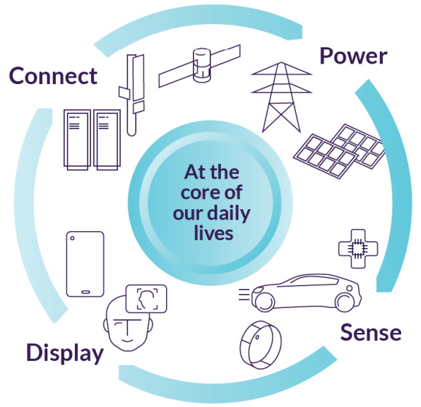
Compound semiconductors are everywhere (Source: IQE)
CONNECT: You want a smartphone that supports 5G, 6G, and links to Starlink satellites? Compound semiconductors support much higher frequencies with much lower power consumption than silicon.
POWER: GaN compound semiconductors underpin highly efficient power electronics, making possible a diverse set of applications, from electric battery charging in automobiles and 5G power amplifiers in phone handsets to underpinning the global drive to NetZero.
SENSE: If your smartphone can recognize your face, it’s using compound semiconductors to handle that 3D sensing task. And compound semiconductors are enabling eye-safe LiDAR for autonomous cars, infrared sensing for defense and industrial, and more.
DISPLAY: MicroLEDs based on GaAs/GaN compound semiconductors can achieve ultra-high density and efficiency, making them ideal for the metaverse, wearable devices, smart displays, and large-scale direct view displays.
Now, this is the point where (a) things get interesting and (b) I reveal the depths of my ignorance, where point (b) may be the driving force behind point (a), depending on your point of view. I’m most familiar with the process of creating regular silicon-based CMOS devices (along with things like Flash memory, which requires a few extra steps). In this case, we start off with a substrate in the form of a wafer made out of silicon. Then we do things like growing a layer of oxide, applying a layer of resist, imaging the resist, removing the unwanted resist, etching the oxide, and doping the exposed silicon (introducing other elements) to create P-Type and N-Type structures in the silicon substrate itself. In this scenario, the only things we end up with on top of the substrate are layers of oxide and metallization.
I had assumed that much the same process was used in the case of compound semiconductors, which just goes to show that Alexander knew what he was talking about when he uttered his “a little knowledge is a dangerous thing” proclamation.
We do indeed start with a compound semiconductor substrate in the form of a wafer. The next step, however, is to use an epitaxy process to deposit layers of atomically engineered films onto the surface of the wafer. We can be talking about tens or hundreds of layers here, where each layer stack is bespoke to each target application. This is where the chaps and chapesses at IQE stand proud in the crowd as the only compound semiconductor manufacturer with a global presence creating the epi-layer stacks on the wafers to form epiwafers, which are then shipped to chip makers (like TSMC, for example).
This is the part that blew my socks off, because we don’t get to dope the compound semiconductor stack; instead, we etch away layers as required. What this means is that the layer stack has to be conceived and implemented in such a way as to facilitate the realization of different types of components using different subsets of the same set of layers. Consider the image below showing the combination of a pseudomorphic high electron mobility transistor (pHEMT) switch and a heterojunction bipolar transistor (HBT) power amplifier (PA), for example:
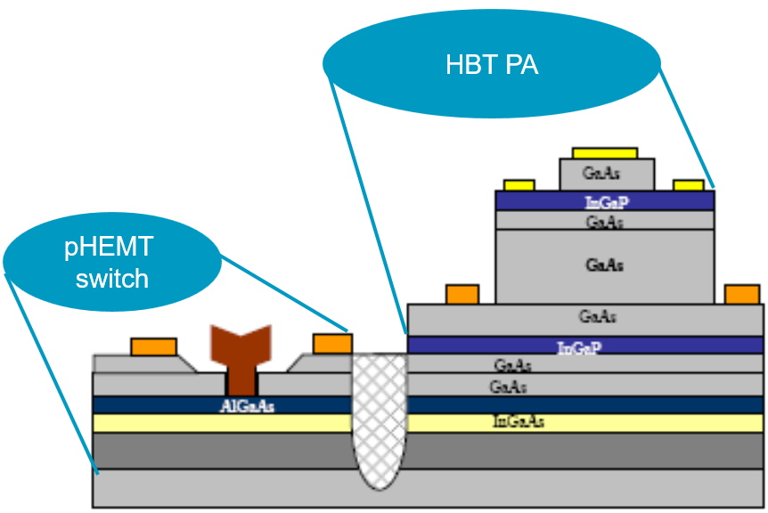
HBT PA and pHEMT switch created using the same epi-layer stack of compound semiconductors
(Source: C. K. Lin, et al., CS MANTECH 2007)
I was still trying to wrap (what I laughingly call) my mind around this concept when Wayne showed me another image that completely blew my socks off. When we had been talking about “using an epitaxy process to deposit layers of atomically engineered films onto the surface of the wafer,” I’d assumed that we were basically growing layers the same way we do with regular elemental semiconductors. For example, if we put a silicon wafer in an oven with oxygen and leave it for a certain amount of time, we end up with a layer of silicon dioxide of a certain thickness. If we increase the time in the oven, we increase the thickness of the oxide. That’s not what we are talking about here. What we are talking about is adding one layer of atoms at a time.
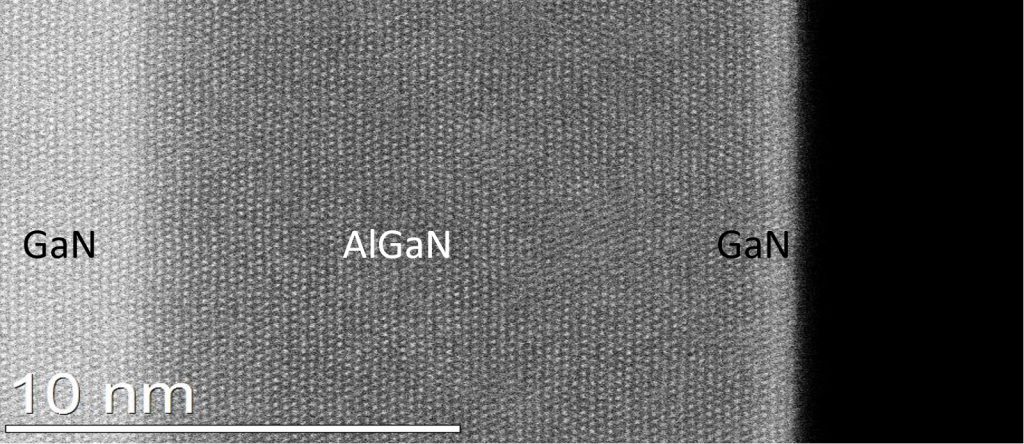
Adding one layer of atoms at a time
(Source: C.-F. Lo et al 2015 ECS Trans. 66 191)
We usually think of wafers as lying flat on a table, but imagine this one as standing up on its edge. What we are looking at here is around 90 or so layers of atoms located at the surface of the wafer. From left to right we see around 16 layers of GaN (the light gray area on the left), then a bunch of layers of ALGaN (the darker gray area in the middle), then 4 or so more layers of GaN (the light gray strip on the right), and then the atmosphere “above” the wafer (the black area on the right). As mind-blowing as this sounds, each of the dots is an individual atom.
“O-M-G,” is all I can say.
While we are mulling over what we’ve just seen, let’s return to the guys and gals at IQE, who would like to leave us with the following thought: “We are the ‘silent enabler’ of the technologies that have become ubiquitous in today’s society. If you have a mobile phone in your pocket, there is a very good chance that it contains IQE material that allows it to communicate with the base station. We were the pioneer in the technology powering 3D sensing that allows facial recognition in high end mobile phones. In addition, the internet as we know it today relies on high-speed data communications enabled by compound semiconductors made by IQE.”
To be honest, they could talk like this for hours—and deservedly so, based on what I’ve seen—but I think we’ll stop here and hand it over to you. What do you think about all of this?


