Investigating the Effects of Cosmic Rays on Space Electronics
 Stefan K. Höeffgen
  Stefan Metzger
 Michael Steffens
- Business Unit Nuclear Effects in Electronics and Optics, Fraunhofer Institute for Technological Trend Analysis INT, Euskirchen, Germany
The radiation environment in space has severe adverse effects on electronic systems. To evaluate radiation sensitivity, electronics are tested on earth with different types of irradiation sources. Cosmic rays (CR) are the most difficult to simulate on earth, because CR can have energies up to 1020 eV, with a flux maximum of around 1 GeV/n. However, only particles with energies up to several GeV/nucleon are relevant for radiation effect testing of space electronics due to the negligible fluxes beyond. Traditionally single-event effects of these particles were simulated with heavy ions having energies of only a few MeV/n because for “large” devices only the energy loss, often referred to as linear energy transfer (LET), had to be matched. Heavy ions of such high energies can produce secondary particles through nuclear interactions which can induce additional ionization that leads to adverse effects. The need to investigate these effects has grown since electronic devices now incorporate heavier elements (e.g., Cu, W) close to sensitive elements which can have significantly larger nuclear cross sections than in the 1 to 10 MeV/n energy regime. At the moment there is a large trend in the space community to increasingly use commercial off-the-shelf (COTS) electronic devices. One of the reasons is that many challenging space applications can only be met with COTS devices because there are simply no space-qualified devices [often referred to as High Reliability (HiRel)] available with the necessary performance. Another trend in the evolution of Si-based microelectronic integrated circuits is to create 3-dimensional (3D) structures. There are already commercially available 3D NAND-Flash devices [i.e., a type of non-volatile computer memory that uses floating-gate transistors that resembles a NAND (NOT-AND) gate] with several tens of active layers stacked on top of each other. These structures cannot be tested with low energy ions, due to the large depths of the sensitive volumes alone. For radiation tests ion beams are needed that provide constant LET over the whole stack (> 128 layers). In addition, e.g., in systems in a package, one finds several dies stacked on top of each in a single package. To investigate the aforementioned device types, the beam has to be able to penetrate through all the dies.
Introduction
The radiation environment in space has severe adverse effects on humans, electronics, and materials. The most challenging part of the environment for our understanding of the effects is related to highly charged, highly energetic (HZE) heavy ions. As with cosmic rays (CRs), these ions can have energies of up to 1,020 eV with a maximum flux at around 1 GeV/n [1].
Only very few facilities in the world are capable of reaching high enough energies to realistically simulate CRs. The only facility in Europe is the GSI Helmholtzzentrum für Schwerionenforschung (GSI) in Darmstadt, Germany, with its heavy ion synchrotron SIS-18, which can reach energies of 1.5 GeV/n. The new heavy ion synchrotron SIS-100 of the Facility for Antiproton and Ion Research (FAIR) will extend this energy beyond 10 GeV/n. With both accelerators a very large part of the CR spectrum will be covered, opening unprecedented research possibilities. The available ion species at FAIR covers antiprotons (for selected experiments) and the whole periodic table from Z = 1 (hydrogen) to Z = 92 (uranium) [2].
Possible space radiation research is foreseen at the BIOMAT cave, operated by the APPA collaboration (Atomic, Plasma Physics, and Applications) [3].
This review looks at the possibilities FAIR offers for research on the effects of galactic cosmic rays on space electronics typically used onboard satellites or future manned space missions. In this review, we conduct an analysis of the open issues in space radiation effects on electronics that would require high energy heavy ions. Finally, some recommendations for a space radiation research program are given.
Open Issues Concerning the Effects of Galactic Cosmic Rays in Electronic Devices
Open issues concerning electronics involving relativistic heavy ions are 2-fold. Firstly there are possible effects in the material that are different for ions of the same LET for higher energy than for lower energy [e.g., single-event effects (SEE) due to nuclear reactions]. Then there are new technologies that simply cannot be tested with low energy ions due to the limited range of the ions.
Dependence of the SEE Cross Sections on Ion Energy
Introduction
The radiation environment in space has severe adverse effects on electronic systems. To evaluate radiation sensitivity, electronics are tested on earth with various irradiation sources. Cosmic rays (CR) are the most difficult to simulate on earth. CR can have energies up to 1,020 eV, with a flux maximum at around 1 GeV/n [1]. For reasons of cost effectiveness and availability, the qualification tests on earth are done at accelerators with much lower energies, usually in the 10 MeV/n range, e.g., at the Heavy Ion Facility (HIF) of the Université catholique de Louvain, Belgium1, or the RADiation Effects Facility (RADEF) of the University of Jyväskylä, Finland2.
The lack of accelerators capable of providing relativistic ions has raised concerns about the fidelity of accelerator-based tests for simulating the response of parts to the real high energy ion environment found in space [4]. Early tests compared the single-event upset (SEU) cross section for ions with a few MeV/n and a hundred or more MeV/n with the same surface LET. They showed either no difference [5–7], or a lower cross section for the high energy ions in the threshold region, where direct ionization is sufficient to induce a SEE [8–10]. This lower cross section was explained by the heavy ion track structure [10]. Ions with higher energy will produce secondary electrons, which have themselves higher energy and can therefore travel farther away from the ion track. Thus, the track radius gets larger for ions with higher energy. This means they deposit less charge in the core area and are potentially less effective than the low energy ions.
More recently, another concern regarding high energy heavy ions has been raised, namely, that of nuclear interactions of high energy ions and the semiconductor materials of which the integrated circuits (IC) are made [11]. Here is an example of the results of a measurement campaign concentrating on high fluence measurements below threshold [12]. A 256 kbit static random-access memory (SRAM) was split into 16 blocks with different feedback resistors to produce different threshold LETs. Figure 1 shows the results for block 3 with a threshold for direct ionization-induced SEUs of about 10 MeVcm2/mg. Low-energy heavy ion irradiations were performed using the tandem Van de Graaff at Brookhaven National Laboratory (BNL) with 11 different ions from C to Au, while high energy heavy ion irradiations were performed at the Texas A&M University (TAMU) heavy ion cyclotron with 5 different ions from Ne to Xe at different energies to result in different LETs. Here even the low-energy ions (10 MeV/n, BNL) produced a low cross section tail of SEUs down to an LET of 1.5 MeVcm2/mg, while the high energy ions (40 MeV/n, TAMU) produce a tail with an order of magnitude larger cross section in the region between 3 and 10 MeVcm2/mg of LET. Calculations have shown that the ion beams at both accelerators have enough energy to exceed the Coulomb barrier and produce Si recoil particles with a maximum LET of about 14 MeVcm2/mg [13]. To further test the assumption of nuclear reactions, a data point was taken with a very low energy (1 MeV/n) carbon beam. Although the beam was able to penetrate several microns deep into the sensitive region, it was not able to exceed the Coulomb barrier and produce recoils [13]. No SEUs have been measured for this data point.
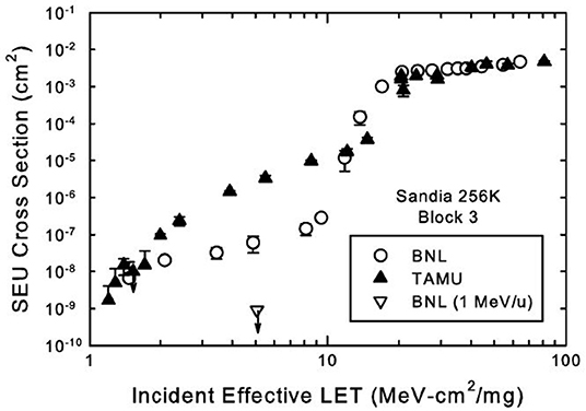
Figure 1. Measured SEU cross section for block 3 of the Sandia 256 kbit SRAM taken with low energy (BNL) and high energy (TAMU) heavy ions [12]. Reproduced with permission from IEEE.
Previous Measurements at GSI
To further investigate the possible influence of high energy heavy ions on electronics testing and to get an answer to the question marks in Figure 2, the European Space Agency (ESA) started a project using high energy beams at GSI [14, 15]. The comparisons were done with the ESA SEU Monitor, which was irradiated at GSI with Fe-56, Ni-58, Ni-64, Au-197, and U-238 ions. The irradiations were done in air and the lid of the chip package was removed.
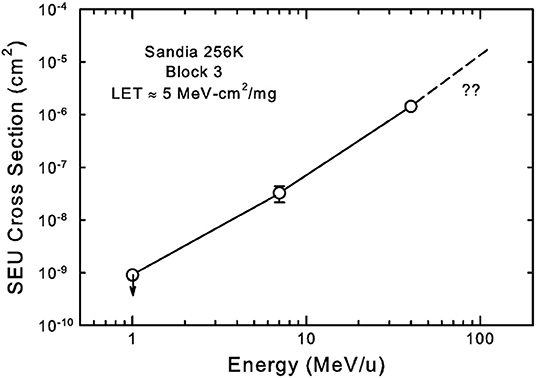
Figure 2. Measured SEU cross section for block 3 of the Sandia 256 kbit SRAM taken with heavy ions having an LET of 5 (MeV cm2/mg) as a function of energy [12]. Reproduced with permission from IEEE.
Figure 3 gives an overview of the results of the irradiations at GSI [14] as well as data taken at RADEF with 6 ions of their standard 9.3 MeV/n cocktail beam [16] and ions of 15 and 25 MeV/n at TAMU [17]. Above the ionization threshold of ca. 4 MeVcm2/mg, there is very good agreement between the GSI (Au-197 and U-238), the TAMU, and the RADEF data. There is no energy effect for ions with similar LET in the range between 10 (RADEF) and 1,000 MeV/n.
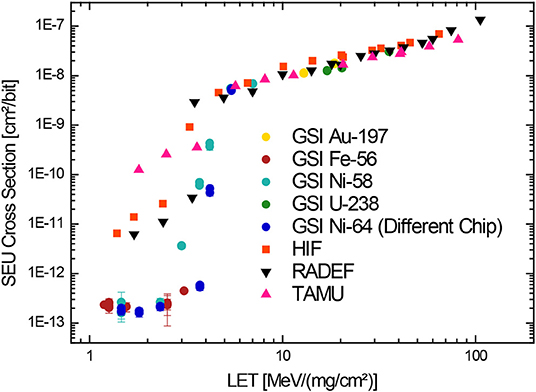
Figure 3. Overview of results measured at GSI, TAMU, and RADEF [14].
A more interesting area is below the threshold region. To emphasize this region, we used a logarithmic x-axis. All data points are based on measured events. So even at 10 MeV/n (RADEF), ions below the ionization threshold are able to produce SEUs. The cross section rises further by over an order of magnitude by increasing the energy of the ions to 25 MeV/n (TAMU). The ions used at GSI were Fe-56, Ni-58, and Ni-64 with energies between 150 and 1,500 MeV/n in the sub-threshold region. The cross section is about two orders of magnitude lower than at 10 MeV/n.
Figure 4 shows the energy dependence for the two different LETs 1.8 and 2.4 MeVcm2/mg. There is an initial increase of the SEU cross section for low energies that was noticed previously in [12]. However, a noticeable decrease of the cross section over nearly 3 orders of magnitude was measured at higher energies of a few hundreds of MeV/n. The authors of [12] did not have access to high energy data and hence they questioned how far this increase would go. At least for the SEU Monitor our data show that the cross section will go down to higher energies. The open question remained as to what the worst-case testing energy for a specific type of chip would be.
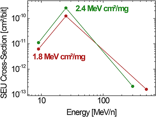
Figure 4. Comparison of energy dependence at specific LET from [14].
There is also a discrepancy within the high energy data for the GSI measurements in the ionizing threshold area (see Figure 5). The Fe-56 and Ni-58 data were taken by Fraunhofer INT using the same SEU Monitor while the Ni-64 data were taken by V. Ferlet-Cavrois (ESA) using a different SEU Monitor. The Ni-64 data seem to have a steeper threshold curve which is also shifted to higher LETs. This is quite surprising because both measurements use the same element albeit different isotopes. The dosimetry at GSI is usually very precise and there is a very good agreement of all data above and below threshold. This fact rules out dosimetry as a possible systematic effect. This leaves chip to chip variations as a possible systematic effect causing the differences between the Ni-58 and Ni-64 data. There is however also a discrepancy between the Ni-58 and the Fe-56 data around an LET of 3 MeVcm2/mg. These two measurements were done using the same chip. This suggests that the effect is due to physical mechanisms not yet fully understood.
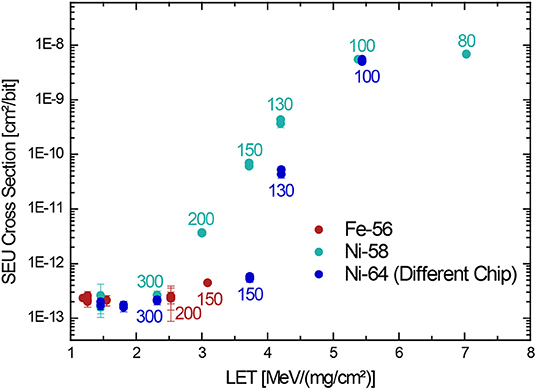
Figure 5. Overview of results measured at GSI, TAMU, and RADEF [14]. The numbers at the data points are the ion energy in MeV/n.
Simulations of the ESA SEU Monitor and New Measurements
As part of their “Radiation to Electronics” (R2E) program, the European Organization for Nuclear Research (CERN) in Geneva, Switzerland investigated energy effects on the SEE cross section of electronics. These investigations also included, in collaboration with ESA, studies on the ESA SEU Monitor [18–21].
They first started with Monte-Carlo simulations, using FLUktuierende KAskade (FLUKA) [21], of the interactions of protons and neutrons (and pions) with the ESA SEU Monitor (see Figure 6) [18–20]. They compared their results of the simulations to the measured cross section at PSI. They found a significant rise of the cross section in the energy range of the protons between 0.3 and 2 GeV. The devices were, as is commonly done in proton irradiations, simulated and irradiated without removing their lid. That means a 420 μm thick layer of Kovar with a gold and nickel plating covered the ESA SEU Monitor.
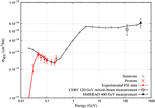
Figure 6. Simulated proton and neutron SEU cross section of the ESA SEU Monitor compared to experimental proton measurements at PSI [19].
Although high energy hadrons are the main concern to electronics in the LHC environment, there were also FLUKA simulations done regarding the influence of high energy heavy ions on the ESA SEU Monitor [21]. The simulations were compared to the measurements previously done at RADEF, HIF, TAMU, and GSI [14], shown in section Previous Measurements at GSI, as well as to new measurements done at the Center for Advanced Radiation Technology (KVI) in Groningen, The Netherlands. Figure 7 give an overview of the experimental data including the new KVI measurements. On the left, the results are shown as a function of LET and on the right as a function of ion energy.
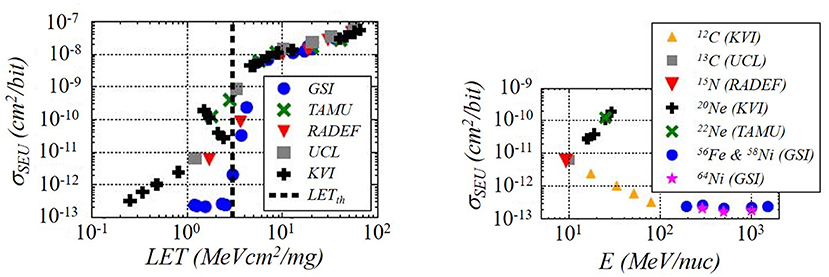
Figure 7. Summary of heavy ion irradiations of the ESA SEU Monitor as a function of LET (left) and energy (right) [21]. Reproduced with permission from IEEE.
The representation on the right of Figure 7 is especially insightful since the LET of the primary ion is not a relevant quantity for effects based on nuclear reactions, as is the case in sub-threshold SEE. This goes one step further than Figure 4, which still compared the energy dependence of the cross sections only for ions having the same LET.
Figure 7 also shows some very peculiar behavior. While the C-13 and N-15 measurements done at HIF and RADEF at 10 MeV/n are fully compatible, the cross sections of the C-12 and Ne-20, both measured at KVI, show a distinctly opposite behavior. The C-12 cross sections decrease with energy and nicely fit the gap between the 10 MeV/n data and the high energy data taken at GSI. The Ne-22 cross section on the other hand increased with energy. The cross section is also fully compatible with the Ne-22 cross section previously measured at TAMU and with energy of 25 MeV/n.
Figure 8 shows the comparison of Monte Carlo simulations with the previous experimental data. The deposited energy in the sensitive volume is provided by the Monte Carlo (MC) Code [either FLUKA or CRÈME MC [22, 23]] and the probability of having an SEU is calibrated to the measured cross section above the threshold.
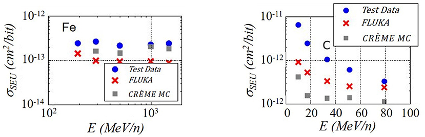
Figure 8. Comparison of FLUKA simulations of heavy ion irradiations of the ESA SEU Monitor with experimental data [21]. Reproduced with permission from IEEE.
For the high energy data on the left of Figure 8, the simulations are within reasonable agreement with the iron measurements done at the GSI. The carbon measurements on the right of Figure 8 show the correct trend, while noticeably underestimating the data. The discrepancies are less for higher energies. It is interesting to notice that the FLUKA simulations are closer to the data for carbon while the CRÈME simulations are closer to the data for iron. In particular this stresses the need to use FAIR to improve the simulation codes for the interaction and transport of particles and nuclei in matter in the corresponding energy range.
Figure 9 shows on the left the FLUKA and CRÈME simulations in comparison to the neon data taken at KVI. Here the simulations underestimate the data up to a factor of 400. Also, the unusual trend of an increasing cross section found in the data cannot be reproduced by simulation. The data from KVI are, as already mentioned, in agreement with measurements at TAMU. In addition, pulse height measurements with a pin diode showed no contamination by other ion species or energies. Also, there is published data, where simulations underestimate the data for 40 MeV/n argon ions by the same margin [24]. The authors of [21] discuss several possible reasons:
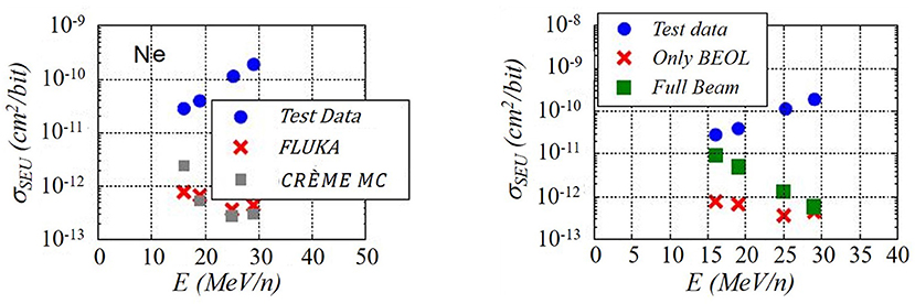
Figure 9. FLUKA simulations of heavy ion irradiations of the ESA SEU Monitor at TAMU (left) and comparison of the cross sections of ions with LET of 1.8 MeV-cm2/mg (right) [21]. BEOL, back end of line. Reproduced with permission from IEEE.
Firstly there could be a material effect. There is no indication that the SRAMs of the ESA SEU Monitor contain tungsten or other heavy elements that have a significant fission cross section [18]. The inclusion of a 50 nm tungsten slab directly above the sensitive volume showed that there are only effects for LET thresholds above 20 MeVcm2/mg, which is much higher than the ~3 MeVcm2/mg of the ESA SEU Monitor.
Secondly, there could be beam size effects. Size effects refer to energy deposition inside the sensitive volume that comes from the space between the edges of the sensitive volume and the edge of the beam. The simulations were done with a beam size of 40 × 40 μm2. An increase of the beam size to 200 × 200 μm2 showed no difference.
Thirdly, there could also be an effect of the beam elements. To account for this the exit window, air, and degraders have been included in the simulation for Ne. The results are shown in Figure 9 on the right as green squares. As can be seen, the inclusion shifts the points somewhat in the right direction but cannot reproduce the increase in the cross section with energy.
Finally, the simulation code could insufficiently describe the nuclear reactions involved. This was reported for similar simulations with GEANT4 [24]. The authors of [24] reported a serious underestimation of the inelastic fragment production energy for the then available models used in GEANT4. The nuclear models of FLUKA on the other hand are used and have been benchmarked for use in medical physics, where a high precision in fragment production energies is important [25]. This stresses again the need to use FAIR to improve the simulation codes as mentioned before.
Open Issues Concerning Energy Effects
There is a very recent publication by the CERN and ESA showing new cross sections for more modern SRAMs containing tungsten in the energy range of several 10s of MeV/n at KVI [26]. These measurements focus on SEL measurements, which have a higher LET threshold and are therefore more sensitive to the effects of nuclear reactions. The result is a consistent decrease of the sub-LET threshold cross section with energy. The cross sections can also be reproduced more or less satisfactorily with integral rectangular parallelepiped (IRPP) Monte Carlo simulations. The increase of the cross section with energy for the ESA SEU Monitor can still be seen for Ne-20, but not for C-12 and O-16. This increase remains an unsolved challenge.
The authors of [26] also extend their simulations to energies in the GeV/n regime and do rate calculations for a CR environment. They calculate even for their most sensitive component, an SRAM containing tungsten with an LET threshold of 15 MeVcm2/mg, only a sub-LET threshold of below 10%. In addition, they claim the rate to be dominated by protons (85%), mainly due to their much higher fluxes. They admit however that for devices with even higher LET thresholds (e.g., above the iron knee at ~30 MeVcm2/mg) for which the high-Z fragments with larger LET could dominate the overall SEE rate. The same goes for packages that introduce a large amount of high-Z material near the sensitive volume [e.g., gold packages discussed in [27]].
Although these predictions are a relief for the space community regarding the hardness assurance, they are mainly based on simulations. A campaign with high energy protons, as well as ions, is needed to verify these predictions.
So far, all investigations of energy effects have concentrated on Si devices (some containing tungsten near the sensitive volume). So far, no results of investigations have been published with SiC or GaN devices, which are increasingly used in power electronics and high frequency devices.
Experimental Needs for High Energy Ions
Beside the need of high energy accelerators for investigating the contribution of secondary particles to SEE, this kind of accelerator has important experimental advantages compared to a low energy one.
Heavy ions with energies of only a few MeV/n have ranges in silicon of only about 100 μm (see Figure 10). Therefore, all irradiations must be performed inside a vacuum tube at the routinely used low energy accelerators. This needs for example a lot of feedthroughs and different electrical connectors. But for the operation of high-speed electronic devices (in the range of hundreds of Mbit/s or above) like in modern double data rate (DDR) 3 or 4 synchronous dynamic random-access memory (SDRAM) the distance between test instrumentation and device under test (DUT) is limited to a few centimeters (typically <10 cm). This is difficult to guarantee at standard installations. For the testing of high-power devices, an efficient cooling system must be provided, particularly when the irradiation should be performed at different temperatures. And when the DUTs are changed it takes a quarter of an hour to proceed with the test because the chamber must be evacuated again.
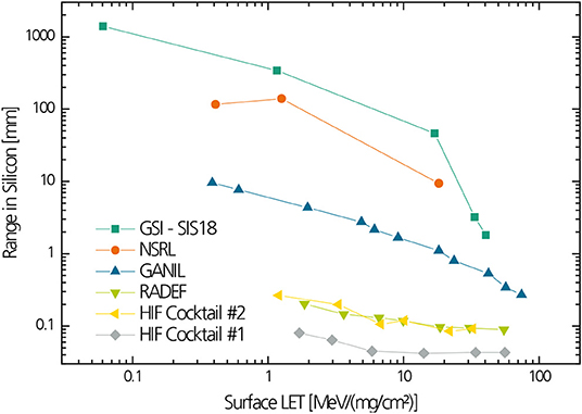
Figure 10. Range in silicon vs. effective LET for several European heavy ion accelerators. Also included is the NASA Space Radiation Laboratory (NSRL) at the Brookhaven National Laboratory.
Another problem of using low energy ions is that the LET varies dramatically inside the DUT and so the energy loss inside the sensitive volume is not the same as at the surface of the device. Therefore, one has to know exactly how the device is assembled to calculate the correct LET value. The problem becomes even worse if one tries to tilt the chip in order to increase the LET or has to irradiate the devices from the backside [28]. In most of the cases of irradiating modern devices with low energy heavy ions the experimenter has to open the chip or to thin it down to a few tens of μm because the range of ions in the semiconductor material is typically less than a few hundred μm (at maximum). So even at normal incidence the ions would not reach the sensitive volume because of their short range. Thinning became more difficult with the advent of new chip packages, e.g., ball grid arrays (BGA), and the increasing number of layers and metallization. Thickness non-uniformity can be rather large and make it necessary to calculate the correct LET for each specific point of the device [28].
Irradiations are usually limited to tilt angles of 60–70°, because otherwise there is too much matter between the beam and the sensitive area. But it can be shown that half of the CR flux hits the device at angles larger than 60° [29]. Here the device might be very sensitive to multiple bit upsets (MBU) along the ion track, which can reduce or even negate the effectiveness of error correction codes.
While a lot of the discussed issues make testing at low energy accelerators more and more challenging, recent technologies can make it impossible (see Figure 11) because the penetration depth of these ions is too small by far. A recent study of a state-of-the-art system on a chip (SOC) devices by NASA showed that thermal problems after opening and removing the heat spreader will limit the use of low energy accelerators [30].
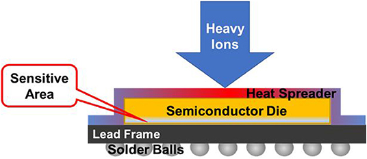
Figure 11. Package of a modern SOC device.
These devices are commonly in a flip chip package with a heat spreader covering one side providing the necessary contact with the heat sink (see Figure 11). This heat spreader forms a layer of copper (300 μm for the Freescale P2020 as an example) on top of the chip, impenetrable for ions from low energy accelerators [31]. Removing the heat spreader completely might damage the device. In [31] it is recommended that the heat spreader is only removed over small areas of the die at a time, while attaching a modified heat sink to the remaining portion. It is foreseeable that this approach can use smaller and smaller areas and will fail in the future.
The current trend in the evolution of Si-based microelectronic integrated circuits is to create 3-dimensional structures. There are already commercially available 3D NAND-Flash devices with several tens of active layers stacked on top of each other (see Figure 12). These structures will be impossible to test with low energy ions, due to the large depths of the sensitive volumes alone. For testing ions are needed that provide constant LET over the whole stack [128 layers as of June 2019 [33], continuously growing]. Because of their commercial availability, 3D NAND-Flash devices could serve as representative components to develop general Radiation Hardness Assurance methods for 3D technologies including new failure mechanisms.
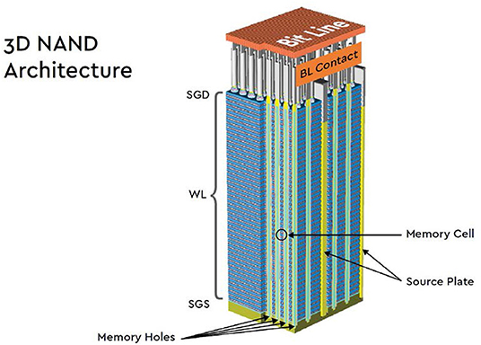
Figure 12. Sketch of a modern 3D NAND FLASH structure architecture from Western Digital [32].
It might be commercially more interesting to test whole boards, systems, or even small satellites, than to qualify every part separately. Because of the high range of the beam, it would be feasible to make a campaign, where a large number of devices are tested simultaneously by stacking several boards. Extending the previous point, whole systems or even small satellites could be tested at FAIR with the 10 GeV/n beam to, e.g., test the effectiveness of mitigation techniques on system level.
Summary and Recommended Research
So far there has only been one campaign to compare the effects of heavy ions of several MeV/n to 1 GeV/n. The device, the ESA SEU monitor, was of older design but very thoroughly characterized at different accelerator facilities. There were some unexpected results that could not be completely answered with simulations of the device. Based on this, a preliminary research program for energy effects on modern Si-based microelectronics should include:
• An extension of the measurements with the SEU monitor up to 10 GeV/n. Although the SEU monitor is of older design, its character as a reference device, that was tested at nearly all relevant accelerators for radiation effects in Europe and that was intensively simulated, makes it a must for any research on energy effects.
• A measurement program similar to the SEU monitor with devices having a higher SEU thresholds (hardened) as well as SEL measurements. SEL is an effect with an intrinsic high threshold (the SEU monitor is SEL free). The devices should contain at least tungsten, possibly also other new materials recently used in novel IC designs. A first step would be comparisons of 10–30 MeV/n, e.g., at RADEF and KVI with 100–1,000 MeV/n at SIS-18 in cave A/M. These could later be extended to energies up to 10 GeV/n at SIS-100 and the BIOMAT cave. This program should help to answer the very relevant question of the magnitude of the energy effects under realistic CR conditions and whether it will be necessary to use very high energy heavy ions for qualification in the future.
Other materials are also already used in other areas than digital microelectronics. Wide band gap materials such as SiC and GaN are increasingly applied in power and high-frequency devices. These materials have a wider band gap and higher density then Si-based devices. It is therefore interesting to investigate the possible influences of the ion energy on these devices regarding the track structure.
A contribution of nuclear reactions to effects in devices can also originate from the packaging. Since the sudden occurrence of unexpected destructive events is a major hardness assurance concern, the influence of the micro environment created by the interaction of the packaging and high energy ions should be further investigated.
Other than the effect of the energy regarding interactions of the ions provided by FAIR, the very high penetration depth of these ions has experimental advantages that could be exploited in the following studies:
• There is a strong interest for using state-of-the-art microprocessors or even system on a chip (SoC) devices in space. These devices have high requirements on cooling. Without a heat spreader made out of copper of several hundreds of μm thickness, the device will be damaged during operation because of excessive heat and by no means can be tested with low energy accelerators. A series of interesting COTS devices could be qualified to choose those that can be used in a space environment. The SIS-18 energies will probably suffice for these tests.
• The current trend in the evolution of Si-based microelectronic integrated circuits is to create 3-dimensional structures. There are already commercially available 3D NAND-Flash devices with several tens of active layers stacked on top of each other. These structures will be impossible to test with low energy ions, due to the large depths of the sensitive volumes alone. For testing, ions are needed that provide constant LET over the whole stack (e.g., 128). Because of their commercial availability, 3D NAND-Flash devices could serve as representative components to develop general Radiation Hardness Assurance methods for 3D technologies including new failure mechanisms.
• It might be commercially more interesting to test whole boards or systems than to qualify every part separately. Because of the high penetrations of the beam it would be feasible to make a campaign where a large number of devices are tested simultaneously by stacking several boards in a row. A first study would be a proof of concept of how many devices could be tested in one campaign.
• Extending the previous point, whole systems or even small satellites could be tested at FAIR with the 10 GeV/n beam to, e.g., test the effectiveness of mitigation techniques on a system level.
Author Contributions
SH, SM, and MS contributed to the design and implementation of the research, to the analysis of the results, and to the writing of the manuscript. All authors contributed to the article and approved the submitted version.
Funding
Part of the work was funded by ESA under Contract No. 4000110709/14/NL/MV.
Conflict of Interest
The authors declare that the research was conducted in the absence of any commercial or financial relationships that could be construed as a potential conflict of interest.
Footnotes
1. ^Available online at: https://uclouvain.be/en/research-institutes/irmp/crc/applications-technologiques.html (accesses July 07, 2020).
2. ^Available online at: https://www.jyu.fi/science/en/physics/research/infrastructures/accelerator-laboratory/radiation-effects-facility (accessed July 07, 2020).
References
1. Stassinopoulos EG, Raymond JP. The space radiation environment for electronics. Proc IEEE. (1988) 76:1423–42. doi: 10.1109/5.90113
4. Stapor WJ, McDonald PT, Knudson AR, Campbell AB, Glagola BG. Charge collection in silicon for ions of different energy but same linear energy transfer (LET). IEEE Trans Nucl Sci. (1988) 35:1585–90. doi: 10.1109/23.25502
5. Ecoffet R, Duzellier S, Falguère D, Guibert L, Inguimbert C. Low LET cross-section measurements using high energy carbon beam. IEEE Trans Nucl Sci. (1997) 4:2230–6. doi: 10.1109/23.659040
6. Koga R, Crain SH, Crain WR, Crawford KB, Hansel SJ. Comparative SEU sensitivies to relativistic heavy ions. IEEE Trans Nucl Sci. (1998) 45:2475–82. doi: 10.1109/23.736488
7. Dodd PE, Musseau O, Shaneyfelt MR, Sexton FW, D'hose C, Hash GL, et al. Impact of ion energy on single-event upset. IEEE Trans Nucl Sci. (1998) 45:2483–91. doi: 10.1109/23.736489
8. Criswell TL, Measel PR, Wahlin KL. Single event upset testing with relativistic heavy ions. IEEE Trans Nucl Sci. (1984) 31:1559–62. doi: 10.1109/TNS.1984.4333548
9. Duzellier S, Falguère D, Moulière L, Ecoffet R, Buisson J. SEE results using high energy ions. IEEE Trans Nucl Sci. (1995) 42:1797–802. doi: 10.1109/23.488781
10. Musseau O, Gardic F, Roche P, Corbière T, Reed RA, Buchner S, et al. Analysis of multiple bit upsets (MBU) in a CMOS SRAM. IEEE Trans Nucl Sci. (1996) 43:2879–88. doi: 10.1109/23.556881
11. Warren KM, Weller RA, Mendenhall MH, Reed RA, Ball DR, Howe CL, et al. The contribution of nuclear reactions to heavy ion single event upset cross section measurements in a high-density SEU hardened SRAM. IEEE Trans Nucl Sci. (2005) 52:2125–31. doi: 10.1109/TNS.2005.860677
12. Dodd PE, Schwank JR, Shaneyfelt MR, Felix JA, Ferlet-Cavrois V, Paillet P, et al. Impact of heavy ion energy and nuclear interactions on single–event upset and latchup in integrated circuits. IEEE Trans Nucl Sci. (2007) 54:2303–11. doi: 10.1109/TNS.2007.909844
13. Reed RA, Weller RA, Schrimpf RD, Mendenhall MH, Warren KM, Massengill LW. Implications of nuclear reactions for single event effects test methods and analysis. IEEE Trans Nucl Sci. (2006) 53:3356–62. doi: 10.1109/TNS.2006.885950
14. Hoeffgen SK, Metzger S, Alpat B, Menichelli M, Desorgher L. Investigation and Analysis of Very High Energy Accelerators for Radiation Simulation. ESA-ESTEC ITT/1-5897/08/NL/JK Final Report. Noordwijk (2011).
15. Hoeffgen SK, Durante M, Ferlet-Cavrois V, Harboe-Sørensen R, Lennartz W, Kündgen T, et al. Investigations of single event effects with heavy ions of energies up to 1.5 GeV/n. IEEE Trans Nucl Sci. (2012) 59:1161–6. doi: 10.1109/TNS.2012.2201502
16. Harboe-Sorenson R, Guerre FX, Roseng A. Design, testing and calibration of a reference seu monitor system. In: RADECS 2005, Proceedings of the 8th European Conference on Radiation and Its Effects on Components and Systems. Agde (2005). p. B3-1–7. doi: 10.1109/RADECS.2005.4365561
17. Harboe-Sørensen R, Harboe-Sørensen R, Poivey C, Fleurinck N, Puimege K, Zadeh A, et al. The technology demonstration module on-board PROBA-II. IEEE Trans Nucl Sci. (2011) 58:1001–7. doi: 10.1109/TNS.2010.2095468
18. García Alía R, Biskup B, Brugger M, Calviani M, Poivey C, Roed K, et al. SEU measurements and simulations in a mixed field environment. IEEE Trans Nucl Sci. (2013) 60:2469–76. doi: 10.1109/TNS.2013.2249096
19. Hoeffgen SK, Metzger S, Brings R, Felden O, Gebel R, Maier R, et al. Past, present and future activities for radiation effects testing at JULIC/COSY. In: Cyclotrons 2013, Proceedings of the 20th International Conference on Cyclotrons and their Applications. Vancouver, BC (2013). p. 88–90.
20. García Alía R, Brugger M, Danezeca S, Ferlet-Cavrois V, Poivey C, Roed K, et al. SEE measurements and simulations using mono-energetic GeV-energy hadron beams. IEEE Trans Nucl Sci. (2013) 60:4142–9. doi: 10.1109/TNS.2013.2279690
21. García Alía R, Bahamonde C, Brandenburg S, Brugger M, Daly E, Ferlet-Cavrois V, et al. Sub-LET threshold SEE cross section dependency with ion energy. IEEE Trans Nucl Sci. (2015) 62:1558–78. doi: 10.1109/TNS.2015.2483021
22. Tylka AJ, Adams JH Jr, Boberg PR, Brownstein B, Dietrich WF, Flueckiger EO, et al. CREME96: a revision of the cosmic ray effects on micro-electronics code. IEEE Trans Nucl Sci. (1997) 44:2150–60. doi: 10.1109/23.659030
23. Weller RA, Mendenhall MH, Reed RA, Schrimpf RD, Warren KM, Sierawski BD, et al. Monte carlo simulation of single event effects. IEEE Trans Nucl Sci. (2010) 57:1726–46. doi: 10.1109/TNS.2010.2044807
24. Reed RA, Weller RA, Mendenhall MH, Lauenstein JM, Warren KM, Pellish JA, et al. Impact of ion energy and species on single event effects analysis. IEEE Trans Nucl Sci. (2007) 54:2312–21. doi: 10.1109/TNS.2007.909901
25. Ferrari A, Sala PR, Fasso A, Ranft J. FLUKA, A Multi-Particle Transport Code Geneva: CERN (2005). doi: 10.2172/877507
26. García Alía R, Brugger M, Ferlet-Cavrois V, Brandenburg S, Calcutt J, Cerutti F, et al. Proton dominance of Sub-LET threshold GCR SEE rate. IEEE Trans Nucl Sci. (2017) 64:388–97. doi: 10.1109/TNS.2016.2628363
27. Turflinger TL, Clymer DA, Mason LW, Stone S, George JS, Savage M, et al. RHA implications of proton on gold-plated package structures in SEE evaluations. IEEE Trans Nucl Sci. (2015) 62:2468–75. doi: 10.1109/TNS.2015.2496288
28. Harboe-Sorenson R, Guerre FX, Lewis G. Heavy-Ion SEE test concept and results for DDR-II memories. IEEE Trans Nucl Sci. (2006) 54:2125–30. doi: 10.1109/TNS.2007.909747
29. Pellish JA, Xapsos MA, LaBel KA, Marshall PW, Heidel DF, Rodbell KP, et al. Heavy ion testing at the galactic cosmic ray energy peak. In: RADECS 2009, Proceedings of the 10th European Conference on Radiation and Its Effects on Components and Systems. Bruges (2009). p. 559–62.
30. Guertin SM. SOC SEE Qualification Guideline, 4th edn. NEPP Electronic Technology Workshop. Greenbelt (2013).
32. Klein A, Harlin S. Western Digital and the 3D NAND Revolution – Understanding 3D NAND Technology and its Future Challenges. Western Digital Technology Brief (2017).
33. Anton S. SK Hynix Starts Production of 128-Layer 4D NAND, 176-Layer Being Developed. (2019). Available online at: https://www.anandtech.com/show/14589/sk-hynix-128-layer-4d-nand (accessed July 07, 2020).
Keywords: single-event effect, space electronics, radiation effects, satellite systems, heavy ion accelerators, cosmic rays (CR)
Citation: Höeffgen SK, Metzger S and Steffens M (2020) Investigating the Effects of Cosmic Rays on Space Electronics. Front. Phys. 8:318. doi: 10.3389/fphy.2020.00318
Received: 31 May 2020; Accepted: 10 July 2020;
Published: 18 September 2020.
Edited by:
Vincenzo Patera, Sapienza University of Rome, ItalyReviewed by:
John Norbury, National Aeronautics and Space Administration (NASA), United StatesDimitris Emfietzoglou, University of Ioannina, Greece
Copyright © 2020 Höeffgen, Metzger and Steffens. This is an open-access article distributed under the terms of the Creative Commons Attribution License (CC BY). The use, distribution or reproduction in other forums is permitted, provided the original author(s) and the copyright owner(s) are credited and that the original publication in this journal is cited, in accordance with accepted academic practice. No use, distribution or reproduction is permitted which does not comply with these terms.
*Correspondence: Stefan Metzger, stefan.metzger@int.fraunhofer.de